|
We have a 108m2 class 10000 clean room, which hosts the following equipments: A high sensitivity Raman spectroscopy system (home built), a BF/DF scanning microscopy system (home built), an EMCCD, tunable solid-state lasers, a supercontinuum, a RTC integrating sphere, high precision motorized translation stages, an optical spectrum analyzer, two monochromators, three optical tables with active isolation, an optical microscope, a stereo microscope, long WD high NA objectives, CCD detectors, an ultralow noise current amplifier, an EDFA, an optical fiber cleaver, a radial polarizer, a He-Ne laser, a lock-in amplifier, an oscilloscope, a multimeter, a hotplate stirrer, a syringe pump, Lumercial FDTD Solutions software, and a variety of light analysis, optics, motion control and mechanics.
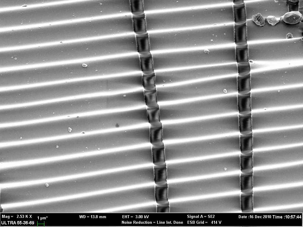
We use the following fabrication and characterization facilities frequently: Electron beam lithography, photolithography, focused ion beam milling, optical fiber fusion splice, scanning electron microscope, atomic force microscope, reactive ion etch, inductively coupled plasma etch, sputtering, eletron beam and thermal evaporation, plasma enhanced chemical vapor deposition, rapid thermal processor, oxidation furnace, chemical mechanical polish, ellipsometer, stylus profilometer, optical profilometer and wire bonding.
We have access to a 56-core processor and the Shanghai Supercompter Center for numerical simulation.
|
|
 |
Rapid and sensitive detection of molecular biomarkers is extremely important in many clinical applications including cancer diagnosis and treatment evaluation, as well as emergent care. The biomarker optical sensing market has been growing as fast as photovoltaics in recent years. However, most of the well-developed bio-optical sensing instruments, to date, are still on the high-end of the market. They are expensive, bulky and require dedicated personnel and lengthy turnaround times to operate, which is unsuitable for point-of-care applications.
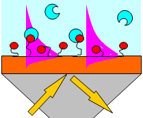
We are developing label-free bio-optical sensing chips which are low cost, compact, portable and high sensitivity. The chips consist of surface plasmon resonance devices on disposable fiber tips, porous materials and microfluidics.
|
|
|
 |
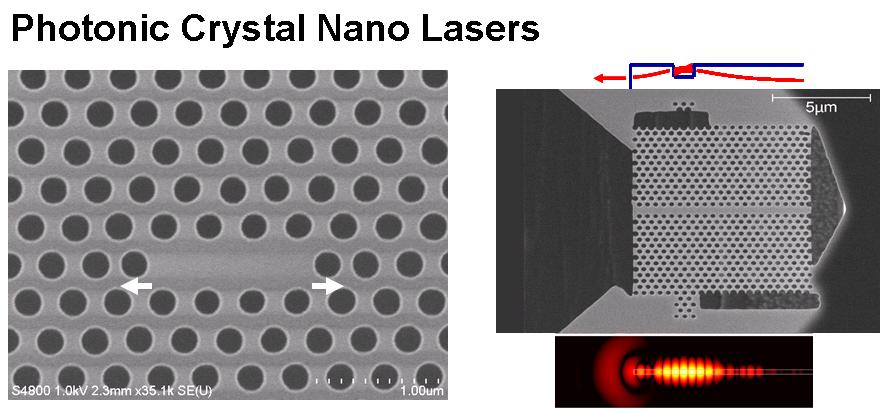
Surface enhanced Raman spectroscopy (SERS) at the single molecule level provides an ultrasensitive and selective method to chemically detect the traces of virtually any materials, and allows the exploration of more detailed information than is available in the spectra taken from a collection of molecules such as molecular dynamics and in situ molecular structural probing. We are developing top-down fabricated nanophotonic devices for well controlled single molecule (non-resonant) Raman spectroscopy.
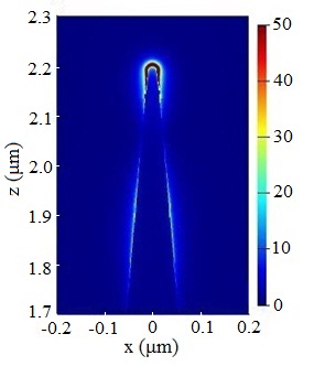
Theoretical modeling indicates strong nanofocusing in a vertical optical antenna integrated with a spiral ring grating, and over 1011 electromagnetic SERS enhancement factors within a 2000cm-1 Stokes shift.
|
|
|
Photonic crystal quantum dot lasers, microdisk InGaSb quantum well lasers on silicon, nanoplasmonic guided-wave theories and DNA identification devices, low-cost fabrication of large-area surface nanostructures by wrinkling, photon management in thin film OPVs and OLEDs
|
|
|
|
|
|